NEWS, EDITORIALS, REFERENCE
Versa64Cart and C64 ROMs

I learned about the Versa64Cart, by Petter Hans (BWACK) over a year ago on Twitter, and the project intrigued me. At the time I knew very little about how external cartridge roms work, but I knew there were a handful of new ROM cartridge boards being made and sold for the C64 and C128, and for the VIC-20 and C16 too.
I love hardware, which is part of the reason why I made the Commodore 8-Bit Buyer's Guide. I continue to work, slowly, on writing reviews of the various projects in the guide, but it's hard for the things that I know little about. Maybe creating the guide was just an excuse for me to get to try everything that's out there. The Versa64Cart was a bit different than some of the others, the PCB, parts list, and documentation are all open source. The buyer's guide lists projects and kits as well as ready-made products, but I like to have a clear understanding of how a regular person can get the final product in their hands. Similarly to 3D printable parts, it's not enough for there to be some spec files, there has to be a clear and easy path to realization. In late 2017, I wrote 3D Printed Components, in which I detail the steps necessary to go from an online catalog of 3D parts, to holding the item in your hands. I want to do the same for the Versa64Cart.
We will get there, I promise. But along the way, it proved to be a somewhat more complicated path to enlightenment. 3D printed keyboard brackets, for example, are pretty easy to use. You stick 'em under your keyboard, put in a few screws, and the keyboard is conveniently positioned correctly. And that's all there is to that. But the Versa64Cart needs the PCB professionally printed, the correct parts list to be ordered, and then everything assembled. But even then, you're not quite done. The Versa64Cart is called "Versa" because it's versatile. It can take EPROM chips of various sizes, which must be programmed correctly with Commodore 64 cartridge software. The versatility allows for multiple binaries to be written into different regions of the same EPROM. The Versa64Cart has 5 jumpers and a bank of 5 dip switches, which must be set correctly for the ROM programs to work.
After getting all the parts and assembling, I also ordered a batch of 32K EPROMs, and then bought the Promenade C1 eprommer that lets me burn EPROMs from my C64. Finally, I set out to do my homework to figure out how this thing actually works, and how the C64's memory mapping extends to support external ROMs. And now, I want to share this whole process, end-to-end, with you.
Let's start with the Commodore 64's memory mapping. This seems fitting, because I just finished writing a post about the 6510 Processor Port. In that post, (if you haven't read it I recommend you do,) I discuss how the port built into the 6510 CPU uses some of its bits to configure the PLA, which is the central hub of the C64's memory mapping. This clever system provides the C64 a great deal of flexibility and expandability.
The C64's Memory Map and the PLA
We saw that the Processor Port's contribution to the PLA has control over 3 main address regions and 5 types of components: The BASIC ROM, the KERNAL ROM, the Character Set ROM, the I/O devices and the RAM that shares those regions. We saw how the processor port selects between components contending for the same shared address range, but what we overlooked is that each component is actually in a specific address range. How does the computer accomplish this? You'll notice, the BASIC and KERNAL ROMs are 2364's, 8 kilobyte chips each. They have only 13 address lines, enough to specify all 8K (2^13 = 8192). The Character ROM is a 2332. It has only 12 address lines, enough to specify its 4 kilobytes (2^12 = 4096). Yet somehow BASIC shows up from $A000 to $BFFF, while the exact same type of chip which houses the KERNAL code shows up from $E000 to $FFFF.
I/O itself is no less mysterious. The region spans from $D000 to $DFFF, but each I/O chip falls at very specific offsets within the region, despite having only a few address lines each. The SID chip, for example, has just 5 address lines, but shows up from $D400 to $D7FF, and the special color memory static RAM from $D800 to $DBFF. The question is, how do they do this? How do these chips find themselves at these specific addresses rather than somewhere else?1
The answer is that the PLA is responsible for all of this. Although the PLA has lots of tricks for mapping different things into the the same addressing regions under different input conditions, the truth is that even if none of those tricks existed, some sort of memory mapping logic array would still be needed to get the ROM chips to appear only within their own narrow address ranges, and the I/O chips to appear in their address ranges, etc.
Let's look at a chunk of the C64 schematic.

Some detail has been removed to make things simpler.
The PLA is the big chip in the middle, U17. The two smaller blocks to the right are actually a pair of 2-bit binary decoders that are found on the same physical chip, U15. Together these two chips perform all of the address decoding and memory mapping of the entire computer. The PLA is labeled as an 82S100, a field programmable logic array.
Eslapion (Francois Leveille) and e5frog (Fredric Blåholtz) have made the PLAnkton, a modern PLA replacement chip. At World of Commodore 2017, Eslapion gave a talk about some of the specific details of the PLAnkton and the PLA. MindFlareRetro (@MindFlareRetro on Twitter,) made a YouTube video, Schooled By Eslapion, encapsulating the talk, and giving some context to why he felt "schooled."
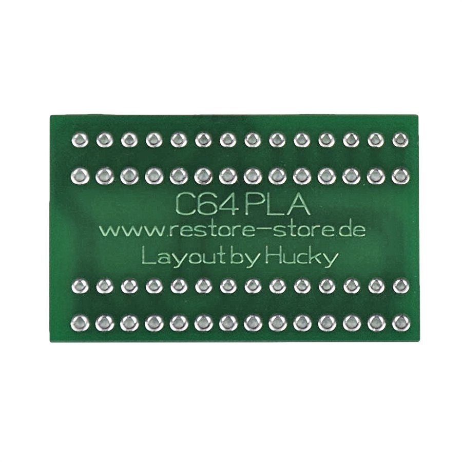
Looking at the 82S100 on the schematic, it appears to be nothing more than a 64K ROM chip. It has 16 input lines (call them address lines), and 8 output lines. Every combination of inputs (all 65,536) has one and only one 8-bit output value. Besides a slight difference in the order of the pins, the PLA seems to be in essence a 27C512 EPROM. MindFlareRetro did some legwork for the rest of us curious folk by making a small board that remaps the pinout of a 27C512 and burning an image of the PLA onto an EPROM. The Buyer's Guide actually lists two such PLA adapter boards, one by Hucky sold by the Restore Store, and the other available from RETRO Innovations.

The problem is, for MindFlareRetro, it didn't work, generating the hilarious Cooooforg 66 corrupted boot screen. Eslapion goes into some detail about what's really going on, which I will very briefly summarize. But, you really should watch the video for the juicy details.
The PLAnkton Saga
Eslapion confirms that the PLA really is just a kind of memory chip. One specific input always results in the same output, there is no registered logic going on inside. However, it's not quite as simple as dropping in any 64K ROM chip, because most ROM chips are not made for this purpose and fail to meet certain timing and signaling conditions present in the 82S100 (and later clones made by Commodore).
The main problem occurs during transitions from one set of inputs to another. While transitioning the output lines contain garbage. In most ROM memory contexts this doesn't matter, but because of the specific requirements of the PLA as the traffic cop of the C64's address bus, any garbage noise during transitions leads to a problem called bus contention, a condition under which more than one thing is signaled that it can use the bus at the same time.
These noisy transitions were detected and confirmed by Eslapion himself by analyzing standard 27C512 EPROMs with some very sophisticated equipment at the university where he was studying electrical engineering, some years ago. There was one exception, a specific version, the M27C512-90B6, which happened to propagate changes to the output more slowly and thus didn't generate intermediate garbage states. This one actually works! And is very cheap, just 1$ USD. Unfortunately the chip is no longer being manufactured, and many that you may find on Ebay are in fact fakes. Intentionally mislabeled chips that, when tested, still exhibit the noise problem.
There are numerous PLA replacements on the market today. All of them that I'm aware of are listed in the Commodore 8-Bit Buyer's Guide. Most are built on modern logic ICs and draw significantly less power than the original. But, the buyer must beware, because some of these chips do not meet the exact timing and other edgy specifications of a real PLA, and can result in glitches that only show up when certain cartridges are used that push the PLA in uncommon, but perfectly legal, ways. The PLAnkton is, at least according to Eslapion, the most faithful and reliable PLA replacement on the market today.
What does the PLA do?
For this, let's bring up the schematic again and take a closer look.
Some detail has been removed to make things simpler.
In the schematic, all of the PLA's inputs run down the left side, while its outputs run down the right. Some inputs and some outputs are missing, because I removed them to make things simpler to understand. Notice how four of the inputs are address bus lines. They are the most significant 4 address lines, A12, A13, A14 and A15. With each next-most-significant address line the address range is divided in two. So, A15 is high whenever an address in the high 32K is being accessed, or low whenever the low 32K is being addressed. A14 subdivides that 32K into two regions of 16K and so on, like this:
| Address Line | Region Size | Number of Regions |
|---|---|---|
| A15 | 32K ($8000) | 2 ($2) |
| A14 | 16K ($4000) | 4 ($4) |
| A13 | 8K ($2000) | 8 ($8) |
| A12 | 4K ($1000) | 16 ($F) |
The PLA, by receiving input from those 4 most significant address lines, knows, at all times, what region of memory is being accessed, down to a precision of 4 kilobyte chunks. The C64 has 16 chunks of memory that are 4K big each. For each of these 16 regions being accessed, the output lines of the PLA can be turned on or off, and these lines connect (generally speaking) to the Chip Select or Output Enable line of a different chip.
The BASIC ROM, to fall between $A000 and $BFFF, has its Chip Select line activated by the PLA when it sees that addresses from either $Axxx or $Bxxx are being accessed. It simultaneously deactivates every other output line, thus disabling every other chip on the bus.
The KERNAL ROM, to fall between $E000 and $FFFF, has its Chip Select line activated by the PLA when it sees that addresses from either $Exxx or $Fxxx are being accessed.
But of course, as we know, BASIC shares its addressing region with RAM and so does the KERNAL and I/O, etc. The PLA doesn't have only those 4 address lines as inputs though. It has the 4 address lines, plus it has all the other inputs, including LORAM, HIRAM and CHAREN from the 6510, as discussed in the previous post, and others that we'll discuss shortly. It is the full value of all its 16 input lines that determines which output line to activate.2
Subdividing I/O Addresses
The PLA sees memory accesses at a fairly coarse grain resolution, one of 16 regions of 4K each. This is enough to activate and deactivate the smallest ROM on the board, the 4K character set ROM. Under different input conditions, instead of activating the 4K character ROM, the PLA will activate the 4K region "I/O" instead. But, I/O isn't one chip. It's a bunch of chips, each of which must have a smaller addressable footprint than 4K. That's where U15 comes in, the pair of 2-bit binary decoders.
Each binary decoder has its own low-active enable line, and takes 2 more next-most-significant address bits and decodes them into 4 separate lines. The way they are arranged is a bit complicated to see at first. The PLA's I/O output line enables the first 2-bit binary decoder, which decodes A11 and A10. These two bits subdivide I/O into four 1K regions, like this:
| A11, A10 | Region Size | Function |
|---|---|---|
| %00 | 1K ($000 to $3FF) | VIC-II |
| %01 | 1K ($400 to $7FF) | SID |
| %10 | 1K ($800 to $BFF) | Color RAM |
| %11 | 1K ($C00 to $FFF) | High I/O |
This first 2-bit decoder is essentially the "Low I/O" decoder. It splits a 4K region into 4 separate 1K regions, but remember that the whole thing is only active when the PLA observes the upper address bits to be in $Dxxx, making these offset from $D000. Thus, the VIC-II ends up at $D000, and the SID at $D400, and Color memory at $D800, very familiar locations to C64 assembly programmers.
The last 1K of the first decoder, however, doesn't activate an I/O chip, it activates another 2-bit decoder, which we can call "High I/O". This second decoder decodes another two address bits, A8 and A9, but in this case it is subdividing a 1K region into 4 regions just 256 bytes big each. Like this:
| A9, A8 | Region Size | Function |
|---|---|---|
| %00 | 256B ($000 to $0FF) | CIA 1 |
| %01 | 256B ($100 to $1FF) | CIA 2 |
| %10 | 256B ($200 to $2FF) | I/O 1 |
| %11 | 256B ($300 to $3FF) | I/O 2 |
Just as Low I/O is offset from $D000, High I/O is offset from $DC00. Thus, CIA 1 is found at $DC00 and CIA 2 is at $DD00. Again, very familiar addresses. The last two High I/O regions, each just 256 bytes big, get offset to $DE00 and $DF00 and are labeled I/O 1 and I/O 2 respectively. What are these for? They don't activate anything on the C64's mainboard, but are instead fed out to lines on the C64's expansion port.
Expansion Addressing
If you're a C64 assembly programmer, you know that the VIC-II and SID have "mirror" addressing locations. Why is that? The VIC-II is activated when the PLA observes $D on A12, A13, A14 and A15, and Low I/O observes $0 on A10 and A11. The VIC-II's own register address lines are then connected to the least significant address bits, A0, A1, A2, A3, A4 and A5.3 As a consequence of this, when the most significant 6 bits activate the VIC-II, and the least significant 6 bits set its registers, there are 4 bits in the middle (A6, A7, A8 and A9) that have no addressing influence. No matter how these are set, the low 6 bits keep talking to the VIC-II. Thus, from a programming standpoint, it is as though the VIC-II's registers are mirrored 16 times.4
Exactly the same phenomenon occurs with the SID chip, only it's slightly more extreme. The SID has 5 address lines of its own, leaving 5 address lines with no addressing influence. This leads to the SID chip appearing to be mirrored 32 times. It happens with both CIA chips too. Each one has 4 address lines of its own, and 8 address lines are required to activate a CIA. Leaving 4 bits without influence, causing each CIA to appear mirrored 16 times.
There is not much we can do about the VIC, SID and CIAs, they are hardwired on the mainboard with this address mirroring arrangement. Although, it has always felt wasteful to me. With a little bit more decoding logic other I/O chips could have been fit in this space, just as the C128 eventually did. The space could even have been left vacant for future expansion options. Regions $DExx and $DFxx, I/O 1 and I/O 2, are designated for external expansion I/O via cartridge. However, in my opinion, cartridges are even more profligate in how they use these two regions. A cartridge will often contain only a single I/O chip, that has very few registers, and yet take up the entire page. For example, the MOS 6551 UART, found in the SwiftLink, has just four registers, it only needs 2 address bits. But these registers are mirrored, making it impossible to combine a SwiftLink with another cartridge on the same I/O page.
Given that the expansion port provides the cartridge with the full address bus, it never made sense to me why they would decode with such coarse grain and then promiscuously use the entire I/O page. However, it all makes sense to me now. The fact is, these cartridges are not doing any address decoding at all. They are relying on the computer's built-in hardware to do all the decoding for them. The I/O 1 and 2 lines are output to the cartridge port alongside the rest of the address bus for a reason. A cartridge merely wires one of the two I/O lines directly to the /CS (low-active chip select) line of its main chip and wires its register lines to the least significant address lines, and its done. The external chip will automatically become active whenever the PLA activates the I/O line it's on. That's the point of the I/O 1 and I/O 2 lines. By relying on these two lines, you don't have to worry about any address decoding. It's all done for you, but at the expense that it isn't quite as fine grain as it could be.
Truth is, the cartridge address usage is not quite as bad as I make it sound. First, a C64 only has one expansion port, so in the early days cartridge creators didn't expect that theirs would have to share the machine with other cartridges. As soon as cartridge port expanders became available, they included options to improve compatibility. X-Pander 3, for example, from Retro Innovations, (like the EX3 and EX2+1 from CMD many years earlier) has jumpers to remap the I/O 1 and 2 lines. Thus, a cartridge hardcoded to I/O 1 can be moved to I/O 2 by crossing the I/O 2 line over to the I/O 1 line on just that port. In this way, two cartridges hardcoded to the same I/O page can be used together.

Green arrows indicate dip switches for disabling individual signal lines on a port-by-port basis.
Red arrows indicate the I/O 1 and 2 swapping jumpers.
This doesn't solve the problem of having more than one cartridge share a single I/O page. However, many cartridges, especially more modern ones, do in fact include some of their own address decoding. The Turbo2325 was the successor to the SwiftLink. Not only was it faster, but it also restricted itself to using only the first 32 bytes of its I/O page, rather than mirroring across the whole 256 bytes.
Some even more modern cartridges take this a step further. The 64NIC+ ethernet cartridge from Retro Innovations and the StereoSID cart by Vanessa Dannenberg, sold by Shareware Plus, include jumpers and dip switches respectively for moving their base address within the page. Thus, it might be possible to get a highspeed RS-232 port, an ethernet adapter, a second SID, and an REU, all sharing a single I/O page. I give that two thumbs up!


Expansion / Cartridge Port Signaling
Now, getting back to the Versa64Cart, let's take a look at what signals are available on the C64's expansion port. (The schematic is presented again, below, so you don't have to scroll half way up the page to refer back to it.)
The expansion port runs along the bottom of the schematic. On the left side we see that cartridges have access to the 8-bit data bus. Following that, we see they also have access to the 16-bit address bus. On the far right of the port we see the lines for I/O 1 and I/O 2, as just discussed, coming down from the High I/O decoder. The data bus can be both input and output, the address bus is usually output, but in some rare situations (using DMA, for example) can also be input. The I/O 1 and 2 lines, on the other hand, are always output.
There are 4 other lines that I've left in the schematic. EXROM, GAME, ROMH and ROML.
Some detail has been removed to make things simpler.
EXROM and GAME go up and into the left side of the PLA. These two lines are input only, and combine with LORAM, HIRAM, CHAREN and the 4 most significant address bits to form part of the PLA's input. As often as not, there will be nothing plugged into the expansion port, which would leave these lines hanging (a state called High-Z, near infinite resistance) which, logically speaking, is neither true nor false. For this reason, these lines have pull up resistors, so they'll go high, and deactivate /EXROM and /GAME when nothing is in the cartridge port.
ROMH and ROML (ROM High and Low) connect to the right side of the PLA. These are output lines, along with the lines for activating RAM, BASIC, the KERNAL and I/O. They don't need need pull ups, because the PLA itself is setting their logical state. They function similarly to the I/O 1 and 2 lines, only for different address regions. They can be connected directly to the /OE (output enable) line of a ROM chip that's in a cartridge, so the cartridge doesn't have to do any of its own address decoding.
When a ROM cartridge is in the expansion port, the cartridge merely has to connect EXROM and/or GAME to ground, thus pulling the lines low. This changes the input pattern on the PLA, informing it that there is an external ROM available. Given that the PLA is just a memory array, any new input can instantly change the PLA's output.
There are 4 possible ROM cartridge modes on the C64: No cartridge, 8K/16K Ultimax cartridge, 8K C64 cartridge and 16K C64 cartridge. To reference 4 modes you need 2 bits. Lo' and behold there are two input bits to the PLA to set the mode. Here's how they work:
| /EXROM | /GAME | Mode |
|---|---|---|
| 1 | 1 | Default, no cartridge |
| 1 | 0 | Ultimax cartridge |
| 0 | 1 | 8K C64 cartridge |
| 0 | 0 | 16K C64 cartridge |
The Extended Memory Map
In the previous post, 6510 Processor Port, we looked at how the memory map is affected by the inputs to the PLA provided by the 6510. That discussion assumed there are no ROM cartridges plugged in. With a cartridge connected, the memory mapping becomes more complex. But, given what we now know about how the PLA works, it's not too complicated.

Based upon the table found at: https://www.c64-wiki.com/wiki/Bank_Switching
Everything in the red block at the top, (no cartridge,) is exactly what we looked at in the previous post. The topmost 8 rows and rightmost 4 columns are nearly identical to the table printed in the book, Advanced Machine Language for the Commodore 64. With the exception that this table includes the range $C000 to $CFFF, which is always RAM.
In the green block, we see the rather radical change in memory map for compatibility with the MAX Machine, also known as Ultimax mode. This mode is identified by the GAME line being activated, while EXROM is deactivated. The MAX Machine only has 2K of RAM, so in this mode the PLA disables everything, including RAM, when the address block is $2 through $7, or $A through $C. I/O is activated when the address block is $D, just like for a regular C64.
You'll notice that the ROM is divided into two distinct regions, ROM LO and ROM HI. ROM LO is from $8000 to $9FFF. That's just before the BASIC ROM, but the BASIC ROM is still turned off, because the MAX Machine doesn't have that ROM. Presumably a MAX cartridge could have two separate 8K ROM chips. The high ROM is in the area where the KERNAL is usually found. A ROM generally needs to be in this area, because the 6502/6510 have their hardware vectors for RESET, NMI and IRQ in the last six bytes of $FFFx.
The code in an Ultimax cartridge expects to be mapped to these memory regions and won't run from anywhere else. But, it is a simple matter for the PLA to activate the ROMH line and deactivate all the other lines (including the KERNAL) when its address lines read either $E or $F, and the EXROM and GAME lines indicate a MAX cartridge is plugged in. It's just a byte stored at that address of the PLA's memory.
In the blue and yellow blocks, a regular C64 ROM cartridge is available. This is characterized by the EXROM line being activated. When EXROM is active, the GAME line distinguishes between an 8K or a 16K ROM.
In a C64 ROM cartridge, low ROM is in the same place as it is in the MAX Machine. It replaces RAM from $8000 to $9FFF, and sits just below BASIC. If only an 8K ROM is plugged in, every other mode that we are now familiar with for patching in BASIC, KERNAL, I/O and the Character ROM, are identical. Program code running in the 8K ROM can patch these in or out using the same INC/DEC $01 trick discussed in the previous post. The only thing to be aware of is that the low ROM is only patched in when the BASIC ROM is also patched in. So, code running from the ROM generally cannot access memory under BASIC.
A 16K C64 ROM cartridge activates both EXROM and GAME. This mode is slightly different in its handling of the BASIC ROM area. The low ROM behaves exactly as when there is only a low ROM available. But the high ROM replaces the BASIC ROM entirely. Plus, there is one additional exception. When BASIC typically gets patched out, but I/O and the KERNAL are left patched in, the high ROM continues to be available where BASIC normally is, but the low ROM gets patched out. The high ROM finally gets patched out when the KERNAL is patched out. I don't know why they chose to do it this way, but that's how it appears to work in the diagram above.
That is the complete extent of the PLA's memory mapping on the C64.
The Versatile Cartridge
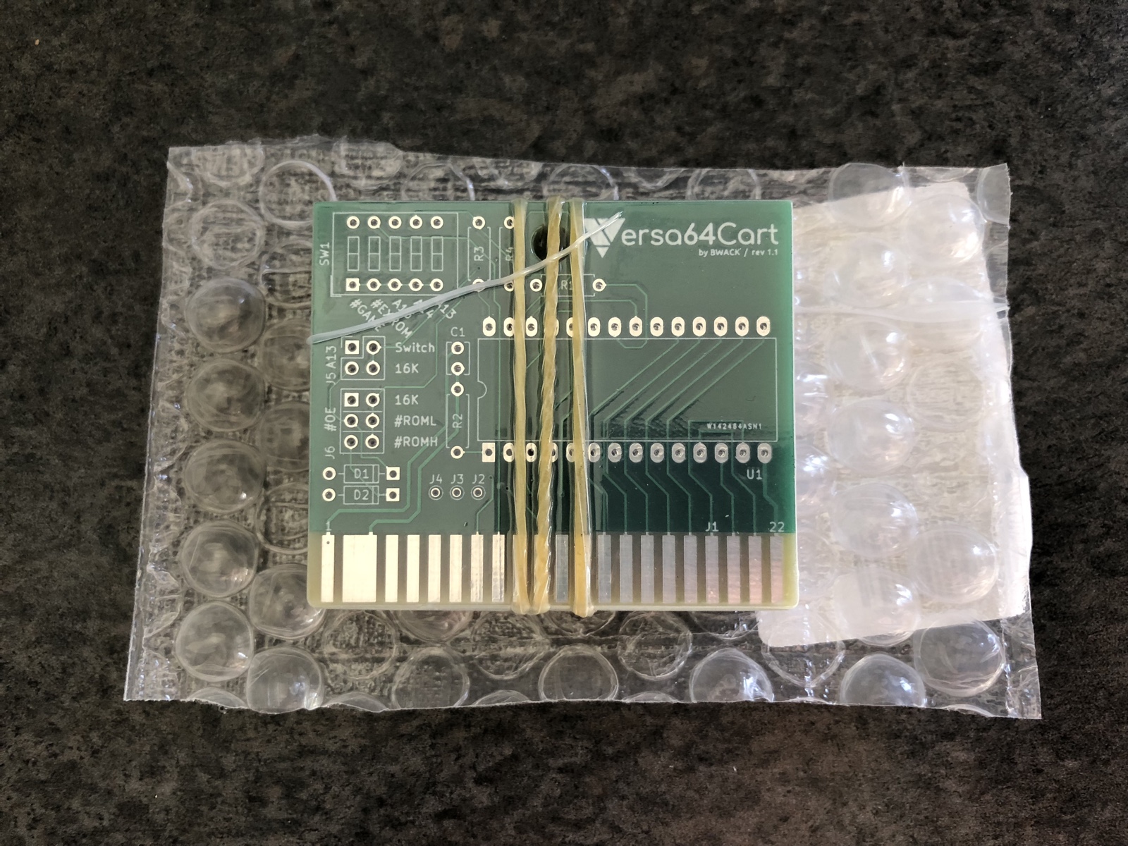
The Versa64Cart can be configured in a number of ways. There are solder pads which can be joined as a cheap way to permanently set a cartridge in one configuration, requiring very few other components. But there are also traces and through-holes where you can solder on jumpers and a dip switch block for easily changing the configuration. Pair this with a socket and an EPROM, and the cartridge can be used as a quick and convenient testbed for a whole host of ROM images.
Here's how the Versa64Cart (v1.1) looks, when fully assembled with all the optional components.
In practice, you'd never have all 5 jumpers closed, but let's take a look at the schematic, and apply some of the information about the PLA and the C64's memory mapping we just learned, to see if we can figure out how this thing works.

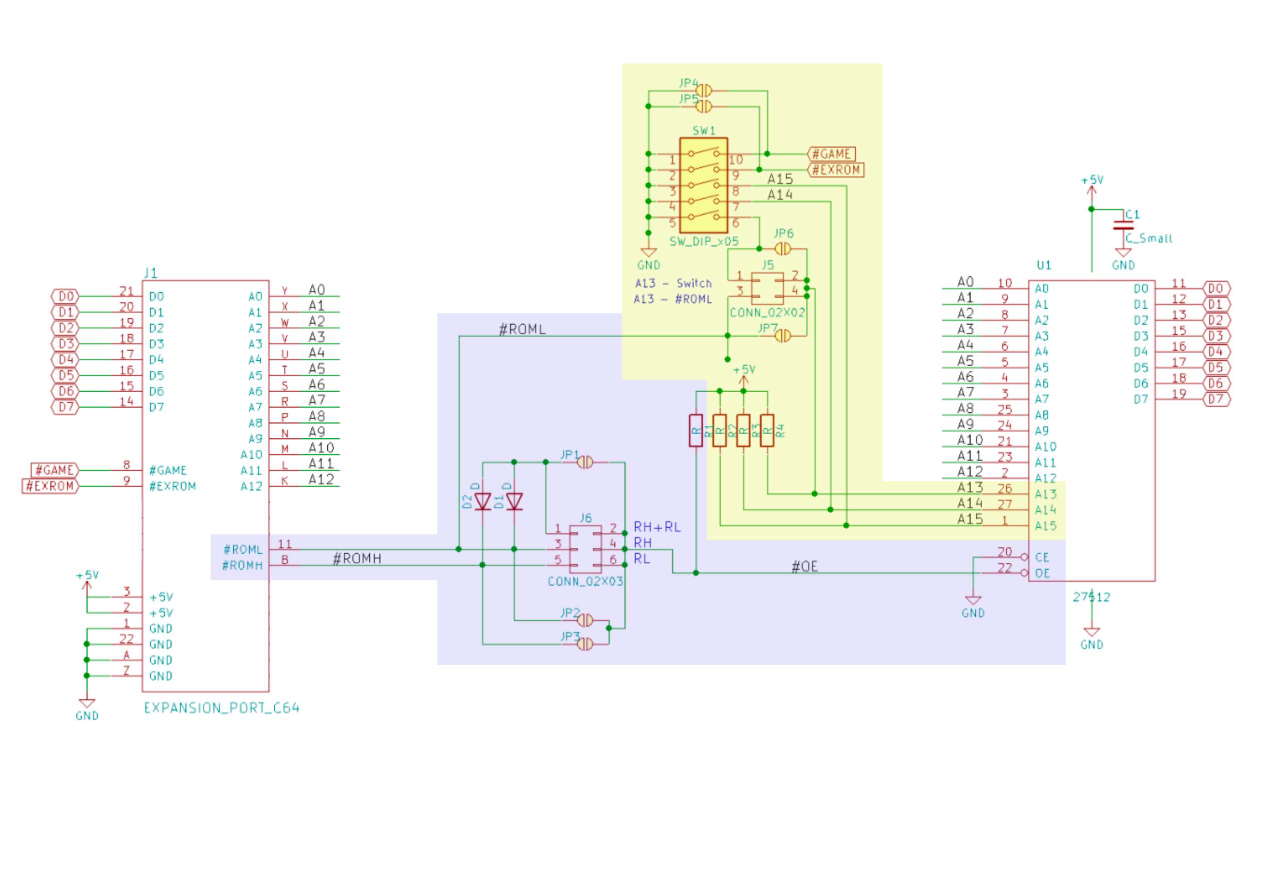
The above right, is zoomed in to show just the schematic and some lines from the expansion port that aren't connected have been removed for clarity. Two regions of the schematic have been highlighted, blue and yellow, to facilitate discussion.
On the left we have the C64's expansion port. And on the right we have a 27512, 28-pin, 64KB, EPROM. Let's look at the simple straight-through connections first. At the top left of the expansion port are the 8 data bus lines. These little labeled lozenges indicate direct connections to the lozenges with the same labels over on the top right of the EPROM. Aka, the EPROM's data pins are wired directly to the C64's data bus. Next, the top right of the expansion port has 13 address lines, A0 to A12. Sans the little lozenge labels, these 13 lines are wired directly to the EPROM's low address lines, from A0 to A12.
Aside: The address lines of any chip must have their least significant bits aligned with the least significant bits of the address bus. For example, the SID chip's 5 address lines must be connected to the address bus's A0 to A4. Imagine what would happen if they were connected from, say, A1 to A5. The address of each register would be shifted one to the left, like this:
| Address Bus | SID Address | Address Value | SID Register |
|---|---|---|---|
| xx00 000x | 00000 | 0 (or 1) | 0 |
| xx00 001x | 00001 | 2 (or 3) | 1 |
| xx00 010x | 00010 | 4 (or 5) | 2 |
| xx00 011x | 00011 | 6 (or 7) | 3 |
| xx00 100x | 00100 | 8 (or 9) | 4 |
As you can see, the low address bit would become meaningless, and each register would be mirrored twice. It would be very strange. Thus, the address lines of all chips on the address bus must align them with the lowest lines on the address bus, which is what we see in the schematic above.
Next, we have all the +5V and GND connections. The bottom left of the expansion port shows which lines are +5V and which are GND, these are connected to all of the other places in the schematic showing a +5V or GND connection. The easy examples are on the EPROM itself. The +5V that powers the EPROM also has a small ceramic capacitor. This is a decoupling capacitor, typically found on the +5V connections of every IC. The C64 itself has such a capacitor on the +5V feed to basically every IC on the mainboard. Digital circuits are sensitive to noise on the supply voltage. A capacitor helps reduce the noise and makes sure the voltage is kept at a steady +5.
Now we come to the trickiest parts of how this works. I've divided the tricky bit into two areas, highlighted yellow and blue. Let's look at the blue section first, as I feel it's a bit easier to understand. At the bottom left of the EPROM are two pins, CE and OE, both are low-active. CE is chip enable, and OE is output enable. Chip Enable is hardwired to ground, so it's always enabled. Output enable determines whether the chip's data lines are available. When output is disabled, the data lines all go to High-Z, causing them to have no logical influence on the data bus.
If we follow the OE line leftward, its first detour is up to a resistor and to +5V. This is a pull-up resistor. If the line were connected to nothing else, then by default it would be pulled up and disable output of the chip. The line is also connected to a block of three jumpers. Each jumper in the block has a corresponding jumper pad in parallel. Whatever you could temporarily set via the jumpers, you could permanently set by soldering across the pads. The whole contraption of 3 jumpers and their alternative pads are wired to just 2 lines on the expansion port: ROML and ROMH.
From what we just learned, ROML and ROMH are controlled by the PLA to activate external ROM chips. Let's take the simple case of an 8K C64 ROM. By closing the RL jumper, the EPROM's output enable will be activated when the PLA activates ROML. That's very cool. This is just as we've been discussing, ROML goes low (aka active) only when the PLA sees $8 or $9 on its 4 address lines, and, via this jumper, is connected directly to the ROM chip's /OE line.
Now how about ROMH? What would happen if we opened RL but closed RH? Well, when ROML is activated, that would not enable the chip. But when ROMH is activated, then the chip would be enabled. If we reference the extended memory map above, this could be used whenever the high ROM is mapped in, assuming it contains code assembled to run from where it's mapped to, and assuming that code doesn't also need to have access to the low ROM. It could be either in the Ultimax address range, $E000 to $FFFF, or the C64 16K cartridge's high ROM range, $A000 to $BFFF. I'm not sure how much software there is out there that would use this arrangement, (high ROM available, but low ROM unavailable,) but the Versa64Cart can easily be configured this way.
How about if we wanted to enable a 16K ROM image?
Here's where things get a bit interesting. Imagine if we had a simple 16K cartridge that contained two separate 8K ROM chips. An 8K ROM chip has only 13 address lines. (A0 to A12. 2^13 = 8192) Thus, each chip would have all of its address lines connected to the low 13 lines of the address bus. Plus, each chip would have all of its 8 data lines connected to the data bus. Then the ROML line would be hardwired to the /OE line of one chip, and the ROMH line would hardwired to the /OE line of the other. Each chip would then be burned with a different image, intended for the memory ranges they would appear at. It's very simple.
However, in the Versa64Cart, there is only one EPROM. That EPROM can be bigger than 8K though. If the Versa64Cart is going to be a 16K cartridge it has to have both 8K images stored in two different 8K banks of a larger ROM. This has important addressing implications that we'll get to next. First, whenever either ROML or ROMH is activated by the PLA the one EPROM chip will need to be output enabled. At first, you might think, oh well, that's easy, right? Just pop a connector onto both RL and RH jumpers at the same time. Unfortunately, you cannot do this.

If you closed both RL and RH, as you can see following the red highlight in the schematic above, you would have a feedback connection from one output line (ROML) back into another output line (ROMH, or vice versa.) And this you simply cannot do.

Instead, if you want a 16K cartridge, open the jumpers RL and RH, and close the third jumper, RH+RL. As you can see in the image above, both ROML and ROMH feed through that jumper to output enable the EPROM. However, there are diodes along those lines that allow voltage to flow in only one direction. When ROML is enabled, voltage can flow through to the chip, but cannot flow back along the ROMH line. And vice versa. A similar situation arose in my NES controller modification, when I wanted the press of the SELECT button to activate both UP and DOWN at the same time. One cannot simply wire UP and DOWN together through the SELECT button's switch, or you get a matrix error. Diodes solved the problem there in exactly the same way as they do here.
Note: If the Versa64Cart is configured in 8K mode only, the diodes do not need to be installed at all.
EPROM Addressing and Banking
Lastly, we'll examine what's going on in the area highlighted in yellow. The schematic is shown again, below, for reference.
An 8K ROM requires 13 address lines, and the Versa64Cart wires those 13 lines directly to the address bus. However, a 16K ROM needs 14 address lines. The C64 supports 16K ROM cartridges, so, why doesn't the Versa64Cart wire all 14 address lines directly to the address bus?
The reason is because in some modes the 16 kilobytes are not contiguous. Therefore the C64 treats the ROMs as two banks that are 8K each. These two banks can be individually activated AND individually mapped by the PLA into different 8K slots in the memory map. In Ultimax mode, as we saw, there is 24K of addressing space between the end of low ROM and the start of high ROM. In order to accomplish this, the PLA activates the two banks with ROML and ROMH, but it gets to choose what higher order address ranges they are activated in.
Before we look at how the addressing works to select the 8K banks, remember that the cartridge needs to signal to the PLA what sorts of ROMs it holds. This is very straight forward via the first two dip switches. We see in the middle left of the expansion port the EXROM and GAME lines with the little label lozenges. These indicate direct connections to the corresponding label lozenges beside the dip switch block at the top of the schematic. When the dip switches are open, these lines are connected to nothing. Recall that the C64's mainboard has pull-up resistors on these lines. If both EXROM and GAME switches are open then both are pulled high and the entire Versa64Cart is disabled. The PLA is signaled that no ROM is available on the expansion port.
The dip switches are connected to ground. Closing a switch pulls the corresponding line low to activate it. There are also jumper pads that can be closed permanently in lieu of the dip switch block. If the EPROM contains an Ultimax game, simply close the GAME switch, but leave the EXROM switch open. If a C64 8K ROM, close the EXROM and open GAME. And lastly, if it's a C64 16K ROM, close both EXROM and GAME.
The remaining three dip switches and 2-jumper block within the yellow highlighted area are responsible for bank selection.
In the 27xxx family of EPROMs the final 2 or 3 digits indicate the number of kilobits of storage. To calculate the number of kilobytes, divide by 8. Like this:
| CHIP # | Kilobits (Kb) | Kilobytes (KB) |
|---|---|---|
| 2708 | 8Kb | 1KB |
| 2716 | 16Kb | 2KB |
| 2732 | 32Kb | 4KB |
| 2764 | 64Kb | 8KB |
| 27128 | 128Kb | 16KB |
| 27256 | 256Kb | 32KB |
| 27512 | 512Kb | 64KB |
The Versa64Cart has a socket for a 28-pin EPROM. The 2764, 27128, 27256 and 27512 are all 28-pin. They are also all pin compatible, as you can see in the diagrams of their pinouts below.


The 8 data lines are on pins 11,12,13,15,16,17,18,19, on all 4 chips. The address lines that are shared between the chips are all on the same pins. The extra address line, A13 on the 27128, takes over a line that is not used for anything on the 2764. The extra address line, A14 on the 27256, takes over a line used for programming the 27128. And the extra address line, A15 on the 27512, takes over the VPP line, which is also used during programming. By doing this, the larger capacity chips are pin compatible with the smaller chips, at least down to 8KB.
There are two ways the C64 needs to access banks on the ROM chip. In 8K mode, ideally, you would want the C64 to be able to use any 8K bank in the chip. So, on a 27C128, a 16K chip, you want to be able to put two 8K programs into the 2 banks, and switch manually between them while configuring the cartridge to report itself to the C64 as being just an 8K cart.
Similarly, if you use a 27C256, you get four 8K banks, and with a 27C512, you get eight 8K banks. And you need a way to specify, manually, which 8K bank you want the cart to use. In this simple 8K mode, you've got the EXROM line active and the GAME line inactive, and you've got the jumper on ROML, (or possibly on ROMH, if you're in that odd situation where you want to use a single 8K ROM as a high ROM without using a low ROM). The bottom 13 address lines are wired straight to the EPROM's low 13 address lines. This gives you up to 3 address lines to set manually. 2^3 = 8 for 8 possible banks, if you're using a 27512 which actually has 8 banks. If you're using a 27256, then the A15 doesn't connect to an address line, and you can just leave it off. And if you're only using a 27128, it doesn't have an A14 either, so the dip switch for A14 doesn't do anything, and you can leave it off. Otherwise, these three switches are used to manually configure the high address lines of the EPROM you're using.
If you look at the EPROM's high three address lines, A13, A14 and A15, you can see that they are pulled up, via three pull-up resistors, to +5V. Thus, if you leave the dip switches off, the lines go high and you are selecting the highest bank. The dip switches connect these lines to ground, so turning a dip switch on pulls the line low for selecting lower banks.
16K Banking
The last and final complication relates to banking of 16K ROMs. Notice that there is a small jumper block with just two jumpers inside the yellow highlighted area. This has two options to let you specify who should control the address line A13. If you configure Versa64Cart for an 8K ROM, you must set this jumper to "switch". This connects A13 to the dip switch so it behaves exactly as I described in the section above.
However, if you are using a 16K ROM, then you've put the jumper in the blue hightlighted area to RH+RL, and you've configured EXROM and GAME for the type either C64 16K or Ultimax, you must also set the A13 jumper not to "switch" but to "ROML." Now, why would that be? Because A13 selects between a high and low 8K bank within a 16K bank. ROML is low-active, so when the computer is addressing ROML that line will activate the EPROM and simultaneously set A13 low to select the low half of the 16K bank. When ROMH is active, ROML goes high (inactive). ROMH activates the EPROM, but the high ROML causes the high 8K bank to be selected. It's like magic!
Now, there is an implication to how this works. If you are using a 27128 none of this really matters as it only has 16K. You can use it as two independent 8K banks, or you can use the whole thing as a 16K ROM that is made up of one low and one high 8K bank. If on the other hand you use a 27256, though, now you've got 32K to play around with. You could use the whole 32K as 4 independent 8K banks. Or, you could use the whole 32K as two 16K ROMs, each with its own 8K low and 8K high ROMs. OR... even more interestingly, you can divide up the 32K so you have two independent 8K ROMs and a 16K ROM.
But here's where you've got to be careful. The 16K ROM must be aligned to a 16K bank. You cannot put onto a 32K EPROM: 8K, 16K, 8K. Because the middle 16K, straddles the split between two 16K banks. Your only choices are as follows:
| 27256 Layouts (256 kilobits, 32 kilobytes) | |||
|---|---|---|---|
| 8K | 8K | 8K | 8K |
| 8K | 8K | 16K | |
| 16K | 8K | 8K | |
| 16K | 16K | ||
Here's an example of a layout that cannot be addressed. Don't do this:
| 27256 Layouts (256 kilobits, 32 kilobytes) | |||
|---|---|---|---|
| 8K | 16K | 8K | |
You are, of course, free to leave any given bank completely unusued. The situation is the same with the 27512, only you've got 64K to work with rather than 32K. 16K ROMs must align with 16K banks.
Configuring the Versa64Cart for 16K is quite easy then. Set J6 to RH+RL. Set J5 to ROML. Then you set EXROM and GAME according to whether the 16K is C64 mode or MAX Machine (Ultimax) mode. And lastly, with a 27256 you can use A14 to toggle between two 16K banks, and with a 27512 you can use A14 and A15 to toggle between four 16K banks. And, be careful when you program your EPROMs where you place your 16K ROMs.
Note: Most jumpers and dip switches have corresponding jumper pads. But the dip switches for A14 and A15 do not have jumper pads. The reason is because if you're going to hardcode the Versa64Cart as an 8K or 16K cartridge, then it makes no sense to use a 32K or 64K ROM. Those extra banks would go unused.
How to get a Versa64Cart
It is harder to get a whole electronic device from nothing but a github download, than it is to get a 3D printable part from nothing but a download. But it is possible, with a bit of effort.
The main component is the PCB. The designer designs the PCB and publishes the project. In this case, Versa64Cart is on GitHub. There are, at this point, a few revisions to the project. 1.1, 1.2, 1.3. Within the folder you'll find gerbers.zip. Gerber files are the standard PCB description files. Download these, but, you can leave the gerber files in the zip archive.

Next, just as you need a source for printing 3D files, you need a service that will "print" PCBs from the gerber files. The recommendation to me, from the 8-bit friendly folk on Twitter, was to use pcbway.com. You have to create an account, but it's free.
From their homepage you'll find a link to get an instant quote. This is where you start. You then have to select from a myriad of customizable options, which at first can be a bit daunting, but can also be quite fun. For example, you get to choose what color you want the PCB to come in, including red, yellow, white and black, among the more standard green or blue. And you get to choose the silkscreen color. So you can make your PCBs look as badass as you want. And you get to choose how many pices you want to order. Here's a difference I found from 3D printing. While it is no problem to order a single 3D printed part, PCBWay has a minimum PCB print of 10. This is not that bad, because even for 10, they only cost about $1.50 each (shipping included!). So this is not a huge outlay.
There are some other parameters, such as PCB thickness, layers, track spacing, surface finish, minimum hole size, etc. that you'll want to get right. Here are the settings I used, on advice from Twitter, for the Versa64Cart PCBs I ordered.

Exactly what the layout of the PCB will be does not factor into the cost. So you'll get your quote on cost of production and shipping cost, which you can add to your cart, before you even upload the Gerber files.
The next stage is where you upload the Gerber files. You just attach the .zip file. This is really great. You don't have to even think about what might be inside that .zip archive.

Lastly, you have to pay. Very straight foward, you can pay with a credit card.
The estimated delivery time is approximately 2 weeks. Mine arrived in less than 2 weeks. And they are absolutely flawless, they come vacuum sealed in plastic. And that is the whole process. It was incredibly easy. We are truly living in the future.
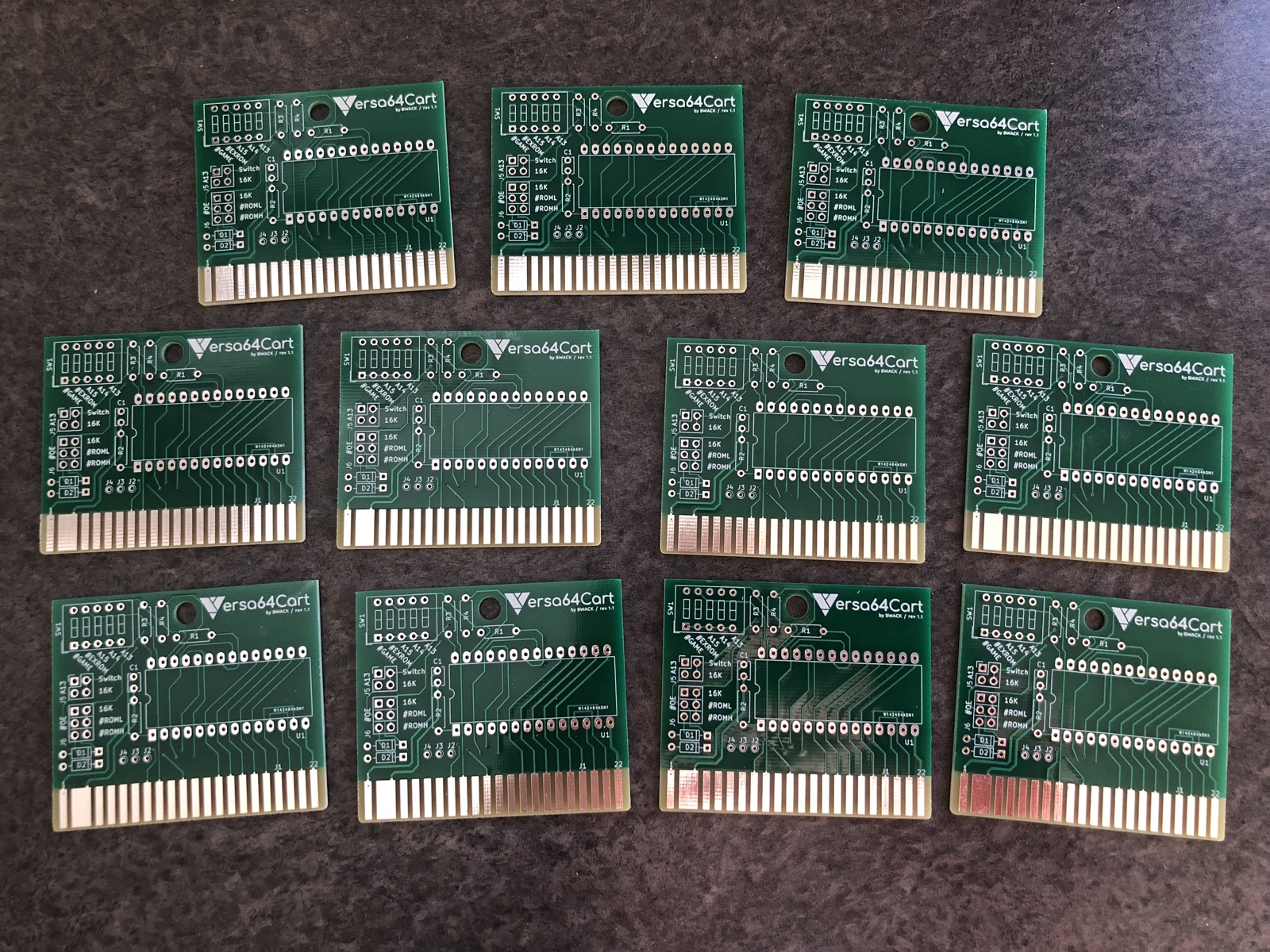
And there they are, 11 beautiful new Versa64Cart PCBs. Wait a second... 11 PCBs? I only ordered 10. That's right, because I'm a new PCBWay customer, they threw in a bonus print for free. That's customer service. I can't guarantee they'll do that for everyone, it might have been a promotion, but it certainly made me happy.
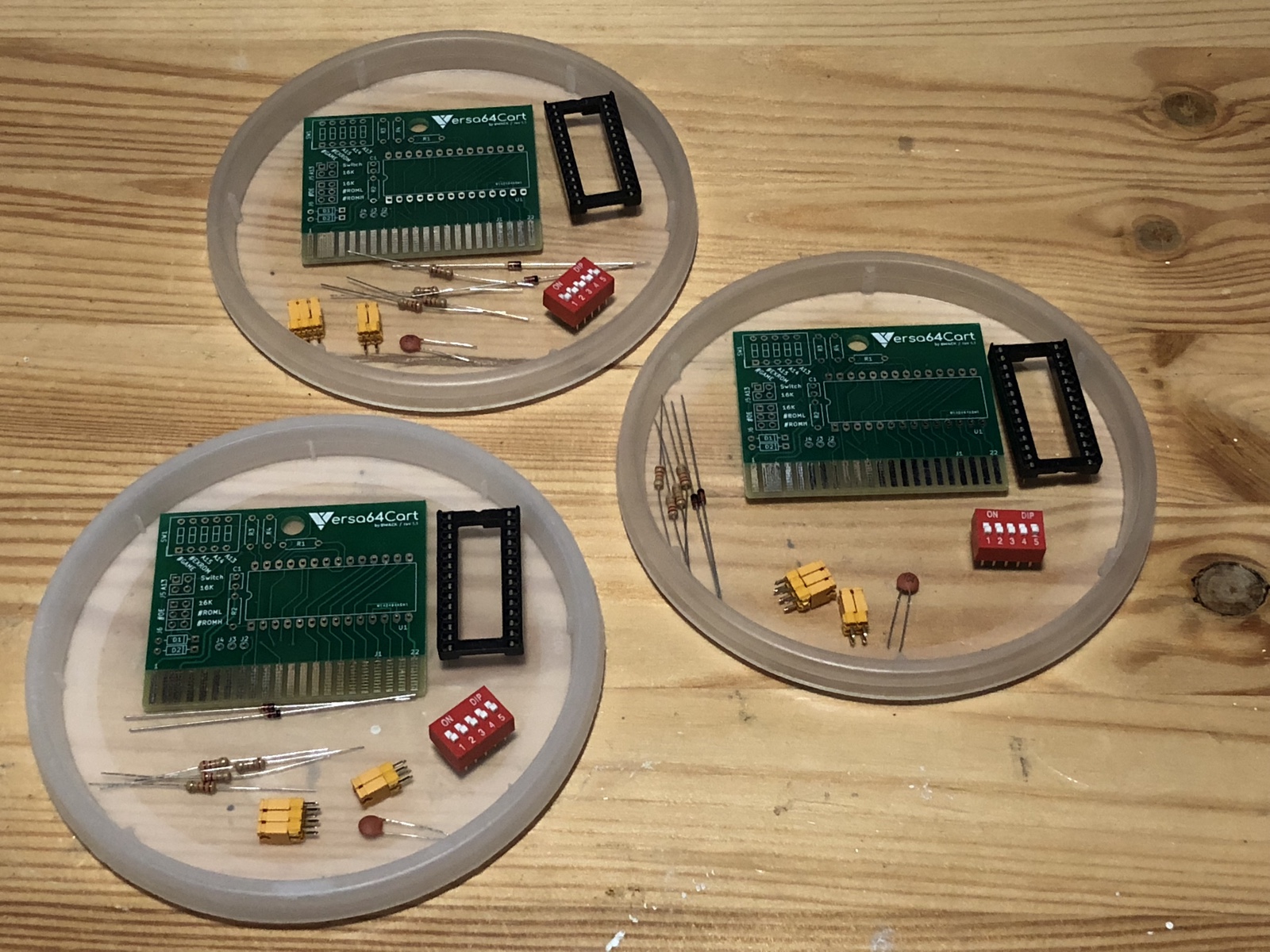
Now, the next task is to gather all of the additional parts. I sourced mine individually from some combination of Amazon and Ebay. No particular trick to doing this, I just looked up each part by name, the parts are listed in the manual that is also available in the GitHub repository. The only thing was that I tried to get the parts in the numbers I needed to match up with the 11 (née 10) PCBs. Some parts, of course, like diodes, you can only buy them in packs of 500 or whatever. These took their sweet time arriving in the mail, as is often the problem with ordering from China through Ebay.

I also ordered a pack of 10 (used, but good condition) EPROMs. I got 27c256's, 32KB EPROMs. These were manufactured in 1986, by AMD. You can alternatively get some modern ROM replacements, such as the ROM-el chips sold by Retro Innovations. These are listed in the Commodore 8-Bit Buyer's Guide in the ROMs section.
You also need some way to be able to program your EPROMs. For this, I managed to buy a Promenade C1, by the Jason-Ranheim company, an EPROM programmer made for the Commodore 64/128 itself. I was super happy to acquire one, as they haven't been manufactured in a long time. This is a topic for another post someday. You can buy USB EPROM programmers for PC/Mac fairly cheaply. But, I have a soft spot for burning them with my C64.


Lastly, you have to assemble them. So, you need a soldering iron and solder. And you need to be able to follow simple instructions.
The only problem is that you'll end up with probably a minimum of 10 Versa64Carts. Maybe you need 10! Maybe you could put 10 games on 10 cartridges and wrap them up in cartridge cases and print out and stick on a sticker. That would be cool.
But, realistically, you probably just want one. So you can play around with it, and test ROMs that you burn, and to generally just be cool.

Buy a Versa64Cart. Support C64OS.com.
But if you don't want to go through that trouble, you can buy one from me, and support my work on C64 OS and C64OS.com in the process.
The Versa64Carts (rev 1.1) use all new parts, are hand soldered and tested by me. They include all of the optional components to make them easily configurable for your own ROMs. Each cart is sold with a 27C256 (32KB) EPROM, and ships in an anti-static bag. Contact me by email if you'd like me to preload the EPROM with particular software.
A color-printed paper manual is included. The cartridges do not include a cartridge case.
Limited availability! Support C64OS.com!
|
|
1 Versa64Cart + 1 EPROM: $20 USD + $7.50 Shipping/Handling OUT OF STOCK!! |
Final Thoughts
I hope this post has been useful and informative. I know I've sat on the Versa64Cart project for many months. But I wanted to get my ducks in a row, and figure out how the C64 makes use of external ROMs. I wanted to have everything in place to test stuff out for myself, so I could write about it all with some authority. And only then would I offer to sell the carts myself.
I really feel like I've leveled up by learning about the PLA and EXROM, GAME and ROML and ROMH lines on the expansion port. It's been a lot of fun.
Keep lovin' your Commodore 64.
- The VIC-II is also an I/O chip whose registers are available from $D000 to $D3FF, but its role in the C64 is much more complicated than almost anything else, and so I will leave it aside, as it's outside the scope of this discussion. [↩]
- Because the ROM chips have a low-active chip select, the PLA activates an output line by pulling it low. For simplicity's sake, I don't talk about the PLA raising or lower an output line. I prefer to say that it activates an output. [↩]
- The VIC-II has 46 registers. 5 bits would only be enough for 32 registers. 6 bits is enough for 64, so it has to be 6 bits. Registers from 46 to 63 are simply invalid. [↩]
- Later machines, such as the C128, use more sophisticated address decoding to put other I/O chips into those mirrored regions. For example, on a C128 in C64 mode, the addresses just above the VIC-II's lowest range is a chip that lets the C64 read the C128's extended keyboard. So, don't use the mirrored addresses. Stick to the base address like the Programmers Reference Guide tells you to. [↩]
- GLINK232 by GGLabs is a 100% clone of the CMD Turbo232, high speed serial cartridge, and is commercially available today. It is listed in the Networking section of the Commodore 8-Bit Buyer's Guide. [↩]
Do you like what you see?
You've just read one of my high-quality, long-form, weblog posts, for free! First, thank you for your interest, it makes producing this content feel worthwhile. I love to hear your input and feedback in the forums below. And I do my best to answer every question.
I'm creating C64 OS and documenting my progress along the way, to give something to you and contribute to the Commodore community. Please consider purchasing one of the items I am currently offering or making a small donation, to help me continue to bring you updates, in-depth technical discussions and programming reference. Your generous support is greatly appreciated.
Greg Naçu — C64OS.com